
Suitable objectives
Surface topography, roughness, step height, morphology, phase contrast, adhesion, and selected mechanical or electrical mapping.
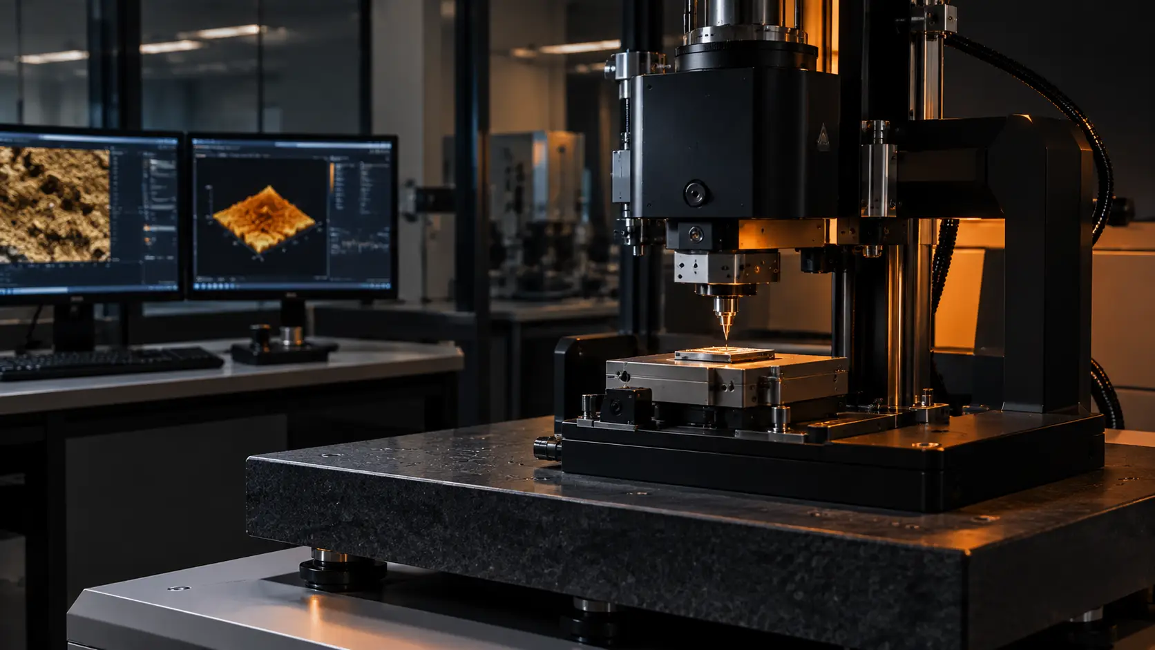
AFM analysis provides nanoscale surface topography and can support roughness, phase, mechanical, electrical, and adhesion mapping in suitable samples. G-Hexa reviews the sample surface, dimensions, measurement objective, and required mode before confirming an AFM analysis route.
Surface topography, roughness, step height, morphology, phase contrast, adhesion, and selected mechanical or electrical mapping.
Thin films, polymers, coatings, semiconductors, ceramics, biomaterials, 2D materials, and other suitable solid surfaces.
Share the surface condition, sample dimensions, roughness expectation, material type, and the property or mode required.
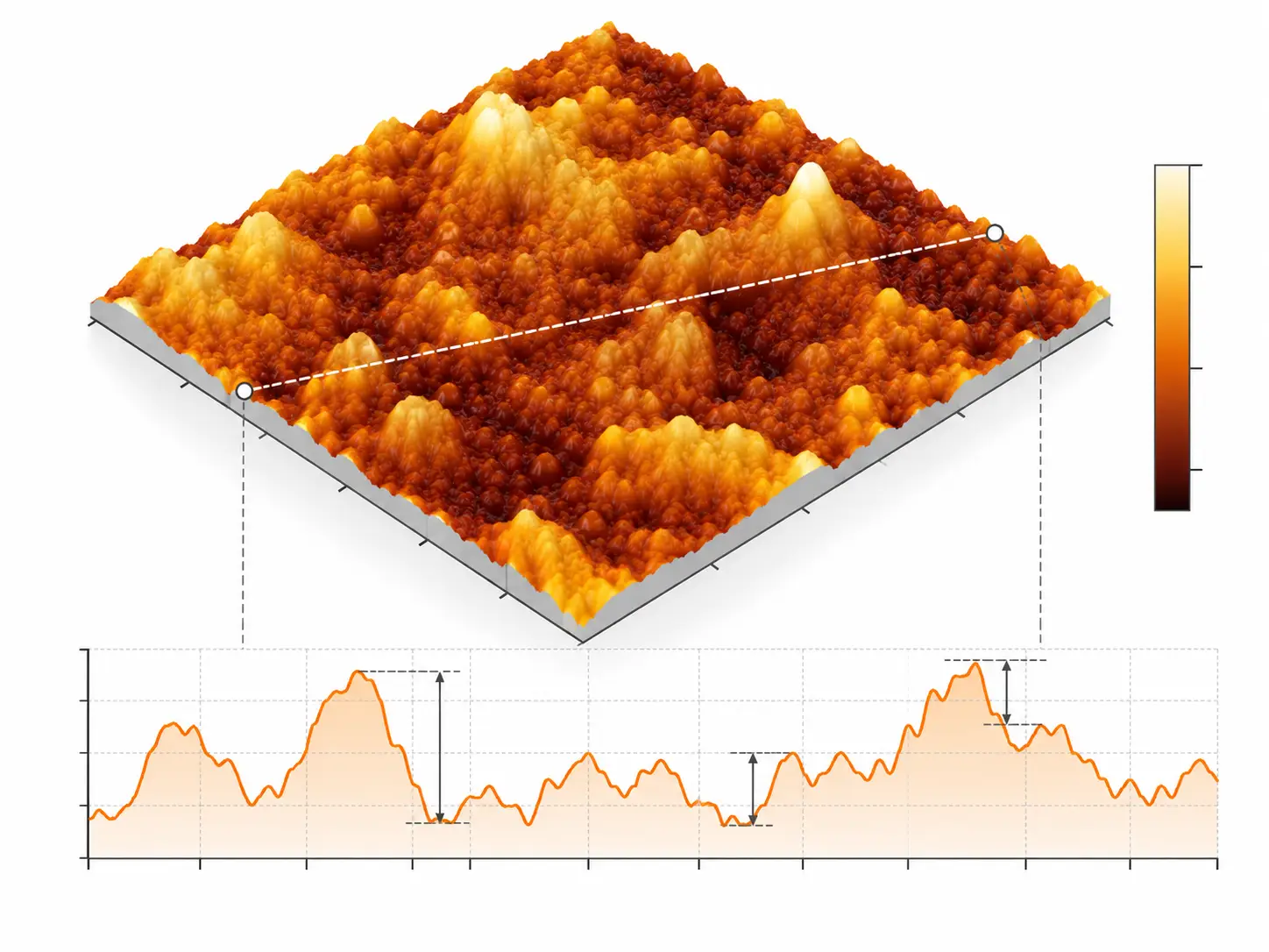
Atomic force microscopy scans a sharp probe across a surface and records the interaction between the probe and the sample. The result can be a three-dimensional topography map or a spatial map of another surface property.
AFM is useful when surface texture, nanoscale features, local contrast, or surface-related properties need to be measured without relying only on optical or electron microscopy.
The appropriate mode depends on the sample surface, probe interaction, environmental conditions, and property you need to map.
Measure nanoscale surface height, morphology, roughness parameters, particles, pits, scratches, and step features.
Investigate local differences in surface interaction, composition-related response, coating domains, and phase contrast where suitable.
Explore local adhesion, stiffness, deformation, or interaction response using suitable AFM modes and probes.
A sharp probe attached to a flexible cantilever scans across the sample surface. Interactions between the probe and sample cause the cantilever to bend or deflect.
A laser and detector system measures that deflection while the instrument feedback system controls the probe position. The recorded signal is converted into a topography or property map.
Tap the probe, surface, detector, or controller to see its role in AFM.
The probe scans a selected surface area, surface interactions deflect the cantilever, the laser and detector measure that response, and feedback control maintains the selected imaging condition. The result is a nanoscale topography or property map.
AFM can quantify nanoscale surface height variation and visualize features such as particles, pits, scratches, steps, wrinkles, pores, and coating texture. The selected scan size and measurement conditions should reflect the feature scale being investigated.
Roughness interpretation depends on scan area, filtering, line correction, sample cleanliness, probe condition, and the measurement parameters agreed for the work.
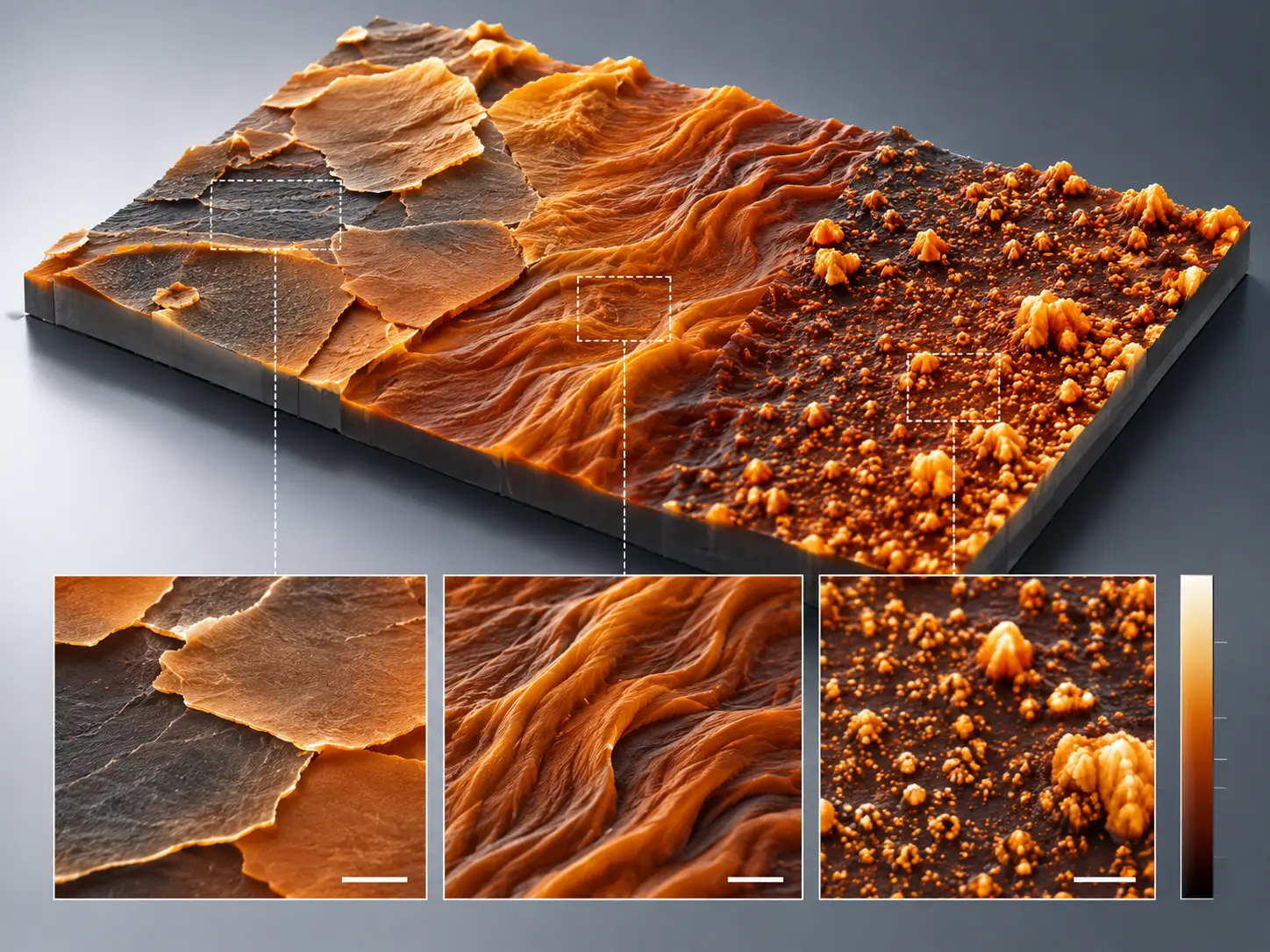
AFM analysis is used when the surface itself contains important information about morphology, processing, roughness, domains, adhesion, or local material response.
Surface texture, roughness, pinholes, domains, defects, and coating uniformity.
Surface morphology, adhesion, phase contrast, deformation, and local interaction response.
Surface steps, roughness, local defects, thin films, and selected electrical or potential maps.
Layer steps, wrinkles, flakes, surface contamination, and nanoscale morphology.
AFM requires a stable, accessible surface and a clearly defined measurement objective. Share the details first so the appropriate mode and probe can be reviewed.
Tell us the material, dimensions, surface condition, target area, and objective.
Our technical team reviews surface accessibility, stability, roughness, and measurement requirements.
Discuss scan size, probe selection, imaging mode, environment, and requested output.
Receive AFM images, roughness data, profiles, maps, and agreed interpretation or documentation.
AFM analysis is used to measure nanoscale surface topography, roughness, step height, morphology, phase contrast, adhesion, mechanical response, and selected electrical properties in suitable samples.
AFM may be suitable for thin films, coatings, polymers, semiconductors, ceramics, biomaterials, graphene, 2D materials, and other solid surfaces that are stable, accessible, and appropriate for probe scanning.
Yes. AFM can generate nanoscale topography and support selected roughness measurements. The result depends on scan area, filtering, probe condition, surface cleanliness, and the agreed measurement parameters.
The suitable mode depends on the sample surface, mechanical properties, required resolution, environment, and property being measured. Contact, tapping, phase, force, electrical, or other modes may be considered after sample review.
Share the material, sample dimensions, surface condition, expected feature size, target area, roughness expectation, and the property or AFM mode you want to investigate. Surface photographs are helpful.
Share a few details for a technical review, or speak directly with our consultant by phone or WhatsApp.
Just a few details — our technical team will guide you.