
Suitable materials
Metals, alloys, powders, ceramics, coatings, polymers, composites, battery materials, and prepared cross-sections.

G-Hexa provides field emission scanning electron microscopy FESEM analysis in India for high-resolution imaging of surface morphology, particles, pores, cracks, coatings, fracture surfaces, and microstructural defects. Our Bengaluru-based team reviews your sample and objective to recommend the appropriate FESEM imaging, BSE contrast, or FESEM-EDS analysis route.
Metals, alloys, powders, ceramics, coatings, polymers, composites, battery materials, and prepared cross-sections.
Surface morphology, particles, pores, cracks, coating defects, inclusions, fracture features, and contamination.
Share your material type, sample dimensions, target area, technical objective, and any handling restrictions.

FESEM analysis is a high-resolution electron microscopy method used to examine a material’s surface and near-surface features. It is commonly used to investigate morphology, particles, pores, cracks, fracture surfaces, coatings, inclusions, and local surface defects.
Secondary electron imaging provides strong topographical contrast, making fine texture, particle edges, micro-voids, fracture features, and surface condition easier to inspect than with conventional optical microscopy.
The recommended mode depends on whether you need surface detail, phase-related contrast, or elemental information from a specific area.
Used for surface topography, fine texture, particles, pores, cracks, coating condition, fracture surfaces, and other morphology-led investigations.
Used to investigate contrast between regions with different average atomic numbers, including phases, inclusions, interfaces, and heterogeneous regions.
Where appropriate, FESEM can be planned with EDS/EDX for elemental identification, point analysis, line scans, or elemental mapping.
A field emission source produces a fine electron beam. Electron optics focus the beam into a narrow probe, while scanning coils sweep it across the selected area of the sample inside a vacuum chamber.
When the beam interacts with the sample, it creates signals including secondary electrons and backscattered electrons. Detectors capture these signals and convert them into high-resolution images.
Tap a component to see its role in FESEM image formation.
The electron source generates a fine beam, electron optics focus it into a probe, scanning coils sweep it across the sample, and detectors convert emitted signals into an image. Secondary electrons emphasize surface topography, while backscattered electrons can provide composition-related contrast.
Backscattered electron imaging can provide contrast between regions with different average atomic numbers. This is useful for examining phase-related contrast, inclusions, interfaces, coating layers, and heterogeneous regions in suitable polished samples.
FESEM imaging primarily provides morphology and contrast. When elemental identification is required, FESEM can be combined with EDS/EDX analysis for suitable elements and sample conditions.
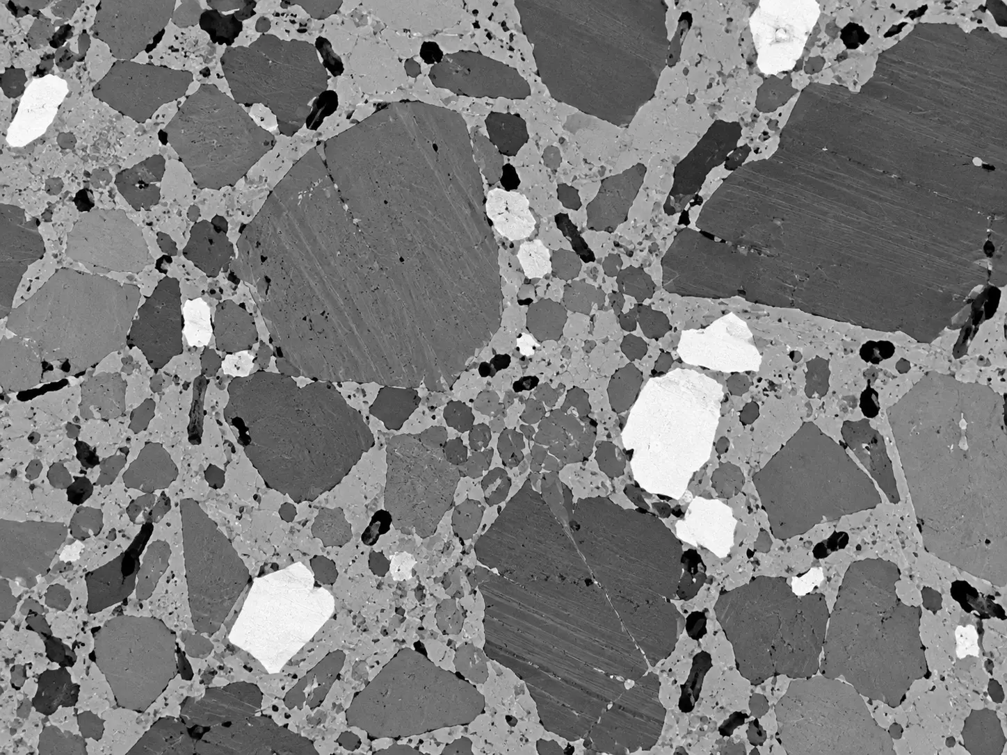
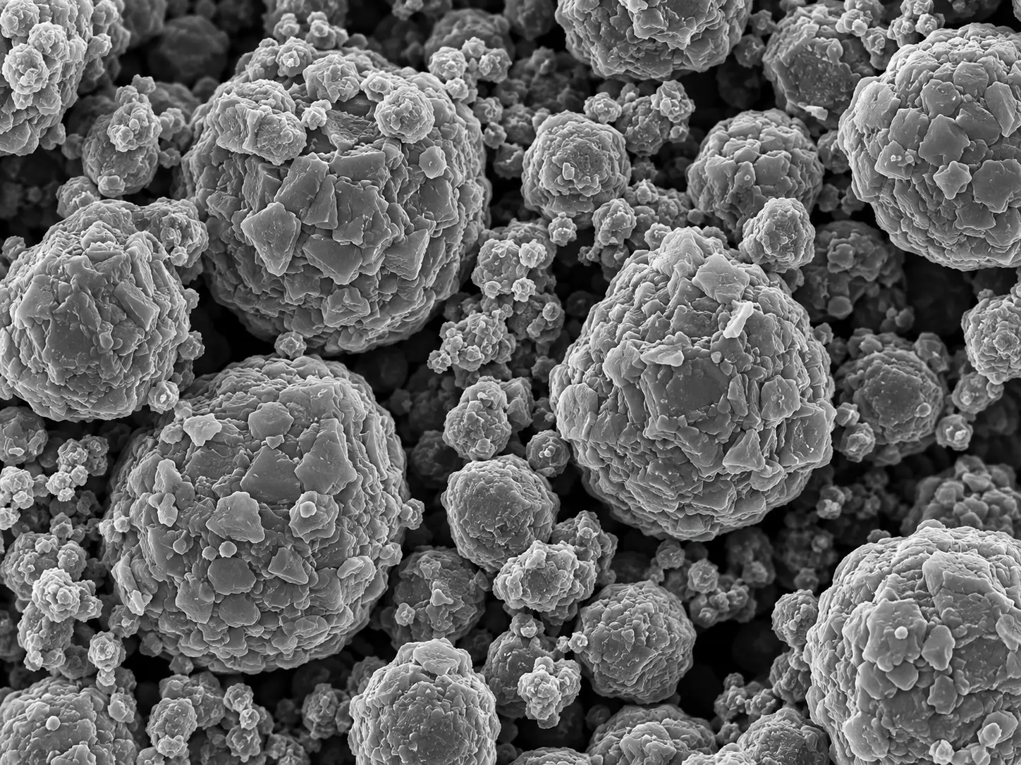
FESEM supports routine materials characterization and focused technical investigations. It can document microscopic evidence during R&D, inspect process outcomes, investigate unexpected defects, and support quality or failure-analysis records.
Fracture features, corrosion products, inclusions, and crack surfaces.
Particle morphology, cracking, agglomeration, and degradation features.
Particle shape, porosity, surface texture, and agglomeration.
Wear, surface defects, delamination, and interface observations.
Share the relevant sample details first. The analysis approach, preparation requirements, and practical submission route are confirmed before dispatch.
Tell us the material type, dimensions, objective, and target region or observed issue.
Our technical team confirms the FESEM route, imaging mode, and any preparation needs.
Send by courier or arrange a drop-off after prior coordination with G-Hexa.
Receive the selected images, observations, and report outputs included in the work plan.
FESEM analysis is used to generate high-resolution images of material surfaces and microstructural features. Common uses include examining particle morphology, cracks, pores, fracture surfaces, coatings, inclusions, corrosion features, surface contamination, and process-related defects.
FESEM uses a field emission electron source that can provide a smaller, brighter electron probe than many conventional SEM configurations. This supports high-resolution imaging of fine surface and near-surface features when detailed morphology is important.
FESEM imaging primarily provides morphology and contrast information. Where appropriate, EDS/EDX can be used with FESEM for elemental identification, point analysis, line scans, or elemental mapping. The appropriate approach depends on the sample and target elements.
Some non-conductive materials may need preparation, such as conductive coating or a specific imaging strategy, to reduce charging effects. The suitable preparation is confirmed after reviewing the sample and your required output.
Share the sample material, approximate dimensions, condition, target feature or defect, analysis objective, and any handling concerns. Clear photographs and marking the target region are helpful when available.
Last reviewed: September 30, 2026
Share a few details for a technical review, or speak directly with our consultant by phone or WhatsApp.
Just a few details — our technical team will guide you.