
Suitable applications
Cross-sections, coatings, interfaces, semiconductor layers, failure sites, thin films, and selected TEM-preparation workflows.
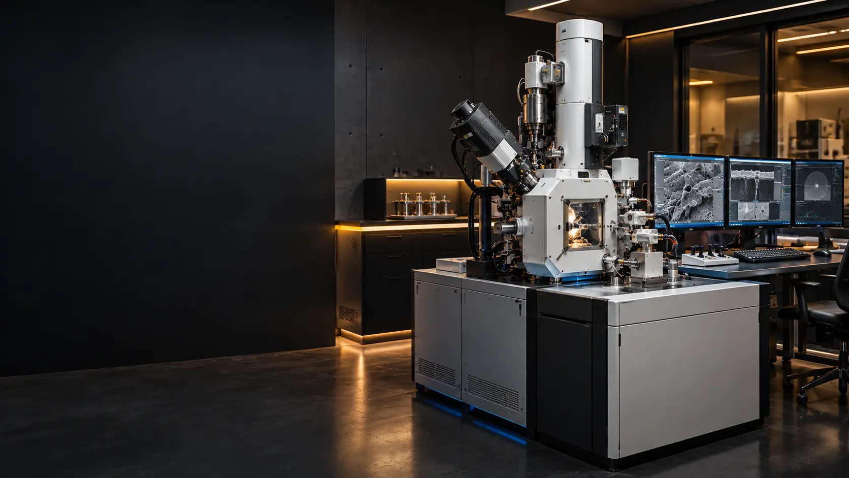
A FIB micromachining service uses a focused ion beam to mill selected regions of a material. It can create site-specific cross-sections, expose buried interfaces, isolate defects, form trenches, and prepare suitable regions for TEM lamella workflows.
Cross-sections, coatings, interfaces, semiconductor layers, failure sites, thin films, and selected TEM-preparation workflows.
Site-specific milling, buried-defect exposure, trench formation, interface inspection, lamella preparation, and controlled material removal.
Share sample photographs, dimensions, target region, material stack, and the analysis you need after milling.
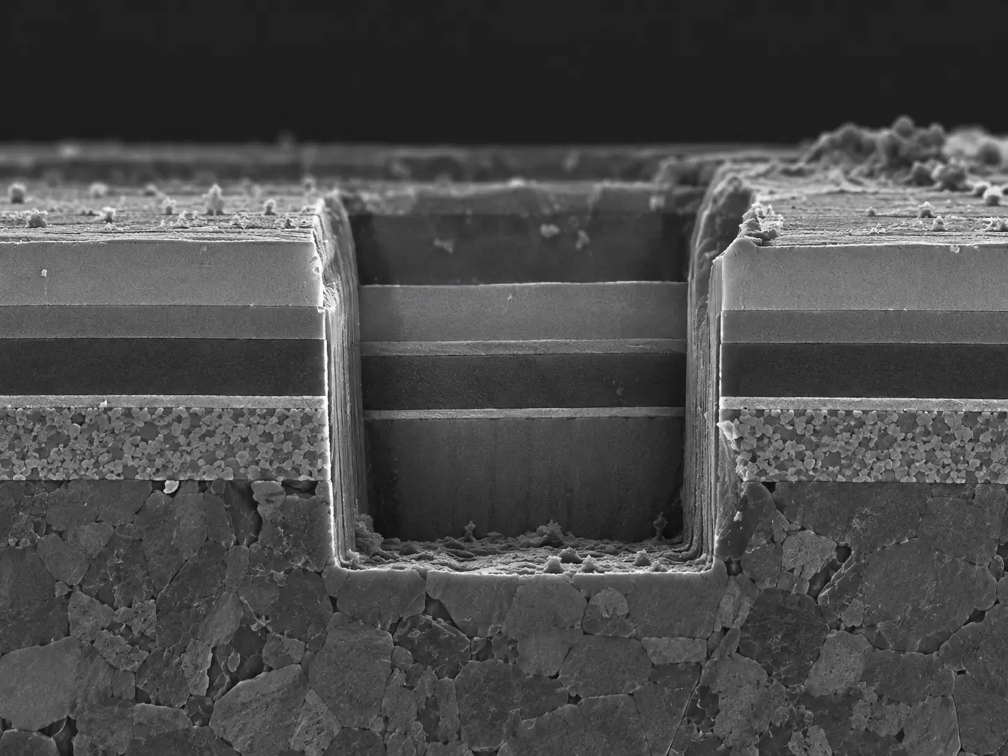
Focused ion beam micromachining removes material from a selected location using a tightly focused ion beam. This makes it possible to expose subsurface layers, isolate a defect, create a trench, or prepare a site for another analytical technique.
FIB is especially useful when the region of interest is small, buried, or difficult to access using conventional mechanical sectioning without damaging the target area.
The suitable route depends on the target region, material stack, desired cross-section, and the analysis that follows the milling step.
Create controlled openings to expose buried layers, interfaces, pores, defects, and site-specific material structure.
Where suitable, prepare a thin site-specific lamella for transmission electron microscopy and nanoscale investigation.
Expose selected failure sites, semiconductor features, coating interfaces, and buried regions for targeted analysis.
A focused ion beam is generated at the source and directed through ion optics toward a selected sample region. Controlled ion impacts remove material from the target site.
The workflow can create a trench, expose a buried interface, isolate a defect, or prepare a thin region for further analysis. Imaging helps document the milled region and guide site-specific preparation.
Tap a workflow component to see its role in FIB micromachining.
The ion source generates the beam, ion optics focus it on the selected region, and controlled milling removes material from the surface. A trench or cross-section exposes the target region, while imaging helps document the milled site and guide the preparation.
FIB can be used for site-specific preparation of a thin lamella when the material, target location, and preparation route are suitable. This allows a selected interface, defect, or buried feature to be prepared for transmission electron microscopy.
Lamella preparation requires careful review of sample geometry, material behaviour, target location, thickness requirements, and protection strategy. The exact preparation workflow is confirmed before work begins.
FIB is used when a specific microscopic region must be exposed, isolated, sectioned, or prepared without relying on broad mechanical removal.
Buried layers, device features, interconnects, and local defect isolation.
Cross-section thickness, interfaces, delamination, and layer structure.
Site-specific exposure of cracks, voids, fracture sites, and buried defects.
Selected lamella preparation for subsequent transmission electron microscopy.
FIB work is planned around the target region and the analysis that follows. Share the details first so suitability and preparation requirements can be reviewed.
Tell us the material, dimensions, target region, layer structure, and objective.
Our technical team reviews the sample and confirms the proposed FIB workflow.
Discuss protection, milling, cross-section, lamella, and imaging requirements where relevant.
Receive the exposed region, prepared specimen, images, or agreed documentation.
FIB micromachining is used for site-specific milling, cross-sectioning, trench formation, buried-interface exposure, defect isolation, controlled material removal, and preparation of selected regions for further analysis.
Yes. FIB can create a site-specific trench or cross-section to expose buried layers, coating interfaces, device structures, voids, cracks, and other subsurface features when the sample is suitable.
FIB may be used to prepare a site-specific TEM lamella when the material, target region, geometry, and preparation requirements are suitable. The workflow must be reviewed before confirming the work.
FIB may be suitable for semiconductor structures, coatings, thin films, metals, ceramics, composites, failure sites, and other solid samples where a specific region needs to be milled or exposed. Suitability depends on size, composition, geometry, stability, and the requested outcome.
Share the sample material, dimensions, target region, layer structure, photographs or drawings, and the analysis required after milling. This helps the technical team plan the appropriate FIB route.
Share a few details for a technical review, or speak directly with our consultant by phone or WhatsApp.
Just a few details — our technical team will guide you.