
Raman objectives
Material identification, phase and crystal-structure analysis, molecular composition, defect studies, and stress or strain mapping.
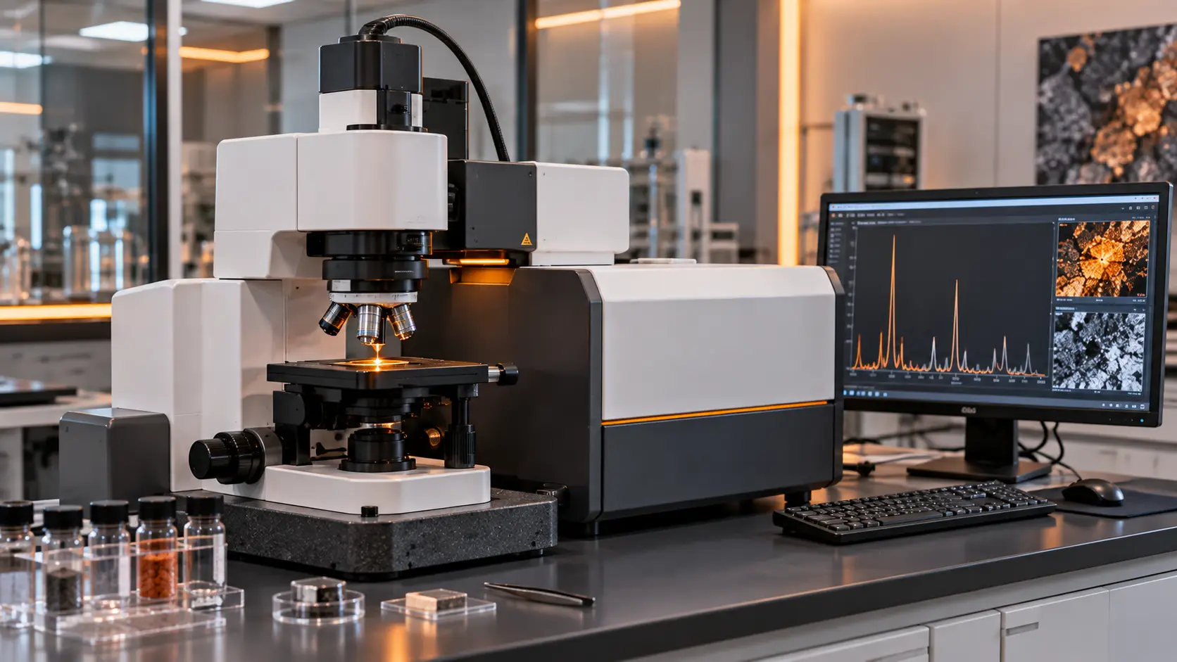
Raman spectroscopy analysis identifies molecular vibrations, crystal structure, phase, defects, stress, and chemical composition by measuring inelastic light scattering. It can support graphene and 2D-material studies, semiconductor analysis, ceramics, polymers, pigments, contaminants, and stress mapping in suitable samples.
Material identification, phase and crystal-structure analysis, molecular composition, defect studies, and stress or strain mapping.
Graphene, 2D materials, semiconductors, ceramics, polymers, pigments, coatings, minerals, and carbon-based materials.
Share the material, sample form, surface condition, expected phases, laser sensitivity, and the chemical or structural objective.
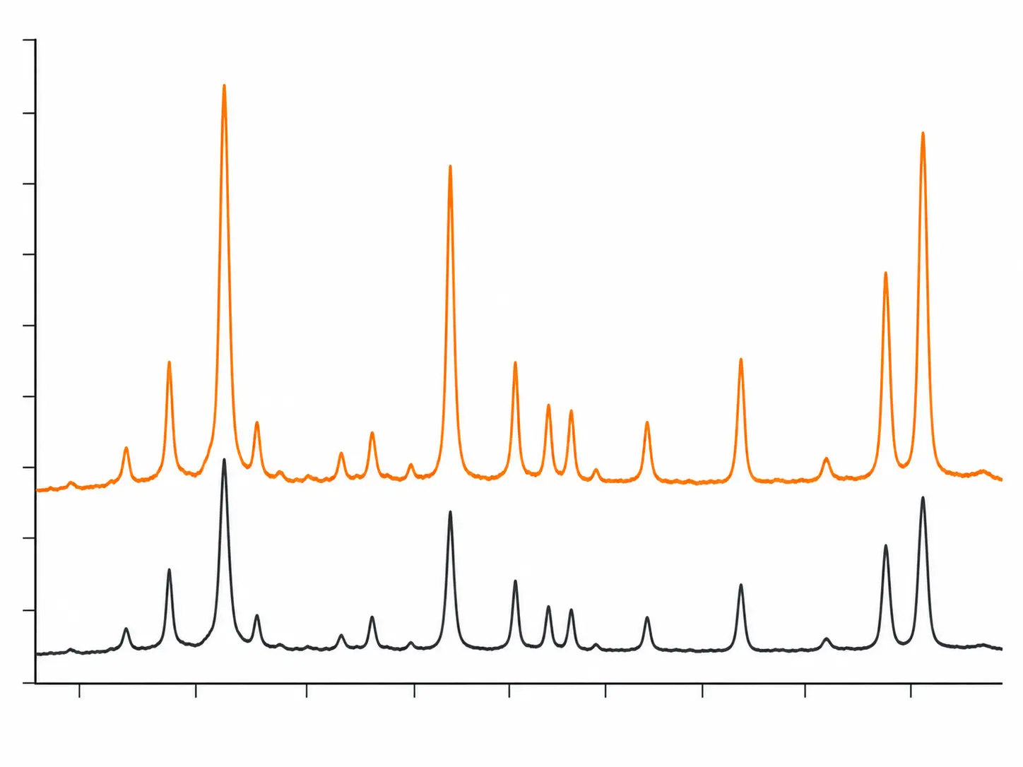
Raman spectroscopy measures the wavelength shift and intensity of light scattered from a sample. The resulting spectrum reflects molecular vibrations, lattice modes, phase, bonding environment, defects, and local structural changes.
Raman interpretation depends on laser wavelength, power, exposure, fluorescence, sample heating, surface condition, spectral range, and reference information.
The appropriate Raman route depends on the material, laser sensitivity, expected spectral features, spatial resolution, and whether identification, mapping, or stress analysis is required.
Compare characteristic Raman peaks to investigate molecular identity, crystal structure, phase, and polymorphic differences.
Investigate D, G, and 2D-band behavior, layer-related features, defects, disorder, strain, and material quality where suitable.
Map Raman peak position or intensity across a selected area to investigate stress, strain, defects, phases, or chemical variation.
A laser is focused onto the sample through a microscope objective. Most scattered light has the same energy as the incident laser, while a small portion undergoes an energy shift related to molecular or lattice vibrations.
The shifted light is separated from the laser line, dispersed by the spectrometer, and recorded as a Raman spectrum for interpretation or mapping.
Tap a component to see its role in Raman spectroscopy.
The laser illuminates the sample, the objective collects scattered light, filters remove the intense laser line, the detector records shifted light, and the resulting spectrum is interpreted for material, phase, defect, stress, or chemical information.
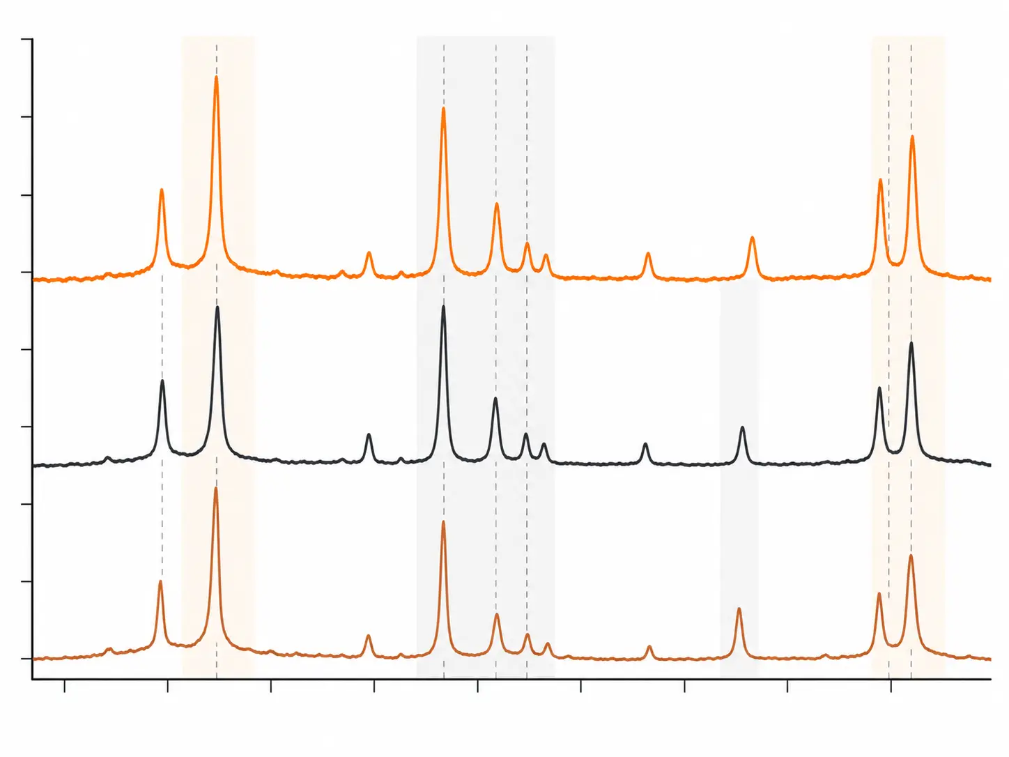
An unknown or processed sample spectrum can be compared with a reference material to identify matching peaks, phase changes, defects, contamination, or changes caused by stress and processing.
Interpretation depends on peak position, intensity, width, fluorescence, baseline treatment, laser wavelength, sample heating, and reference quality.
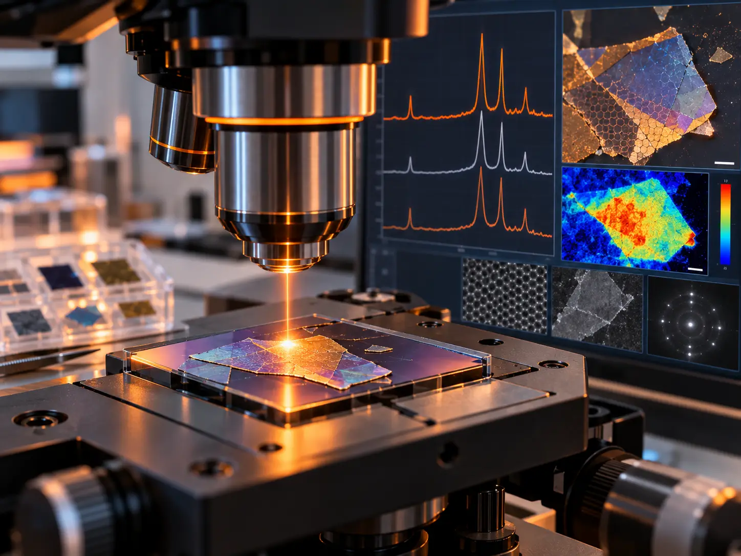
Raman is used when molecular vibration, crystal structure, phase, defects, stress, or spatial chemical variation is central to the investigation.
D, G, and 2D bands, layer-related behavior, strain, defects, disorder, and material quality.
Crystal quality, stress, phase, defects, local heating effects, and spatially resolved material response.
Phase identification, crystal structure, polymorphs, inclusions, and transformation behavior.
Molecular identification, formulation comparison, degradation, additives, and pigment characterization.
Raman planning depends on sample form, fluorescence, laser sensitivity, surface condition, expected chemistry, and the required spatial or spectral output.
Tell us the material, sample form, dimensions, expected phase, and analytical objective.
Our technical team reviews fluorescence, laser sensitivity, surface condition, and expected signal quality.
Discuss laser wavelength, power, scan area, mapping, reference comparison, and requested outputs.
Receive Raman spectra, peak observations, maps, comparison results, and agreed interpretation or documentation.
Raman spectroscopy is used for molecular and material identification, crystal-structure and phase analysis, graphene and 2D-material studies, defect analysis, stress mapping, and spatially resolved chemical or structural investigations.
Raman may be suitable for graphene, 2D materials, semiconductors, ceramics, minerals, polymers, pigments, coatings, powders, crystals, and other samples that produce a usable Raman signal under suitable laser conditions.
Raman can support unknown-material identification through characteristic peak positions, intensities, widths, phase-related features, and comparison with reference spectra. Confidence depends on sample quality, fluorescence, laser conditions, and reference information.
Raman can support stress or strain investigations when the material has a measurable peak response that shifts or changes with local stress. The approach depends on calibration, material system, laser conditions, and reference state.
Share the material type, sample form, dimensions, expected phase or chemistry, surface condition, fluorescence or laser-sensitivity concerns, and whether you need identification, mapping, defect, or stress analysis.
Share a few details for a technical review, or speak directly with our consultant by phone or WhatsApp.
Just a few details — our technical team will guide you.