
Suitable materials
Nanoparticles, catalysts, battery materials, thin films, polymers, ceramics, metals, semiconductors, and electron-transparent specimens.
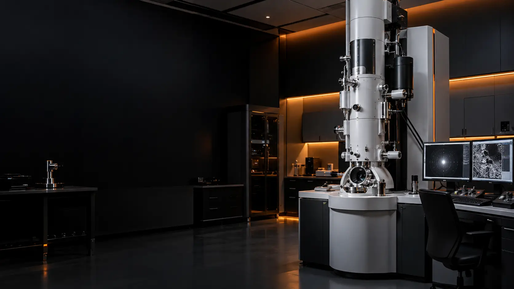
G-Hexa provides TEM analysis in India for imaging nanoparticles, crystalline structure, lattice fringes, interfaces, defects, and nanoscale features. Our Bengaluru-based team reviews your sample and objective to recommend the appropriate TEM, HRTEM, diffraction, or complementary analysis route.
Nanoparticles, catalysts, battery materials, thin films, polymers, ceramics, metals, semiconductors, and electron-transparent specimens.
Particle structure, crystallinity, lattice fringes, interfaces, defects, agglomeration, diffraction, and nanoscale morphology.
Share your material type, expected feature, sample condition, dimensions, and objective so TEM suitability can be reviewed.
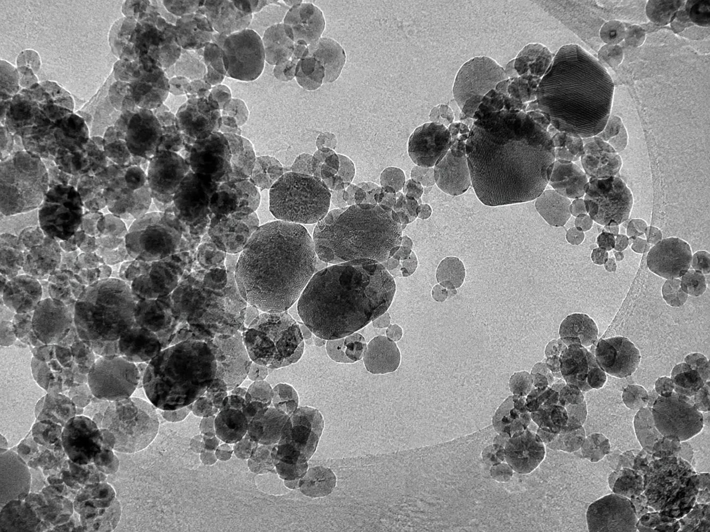
TEM analysis uses transmitted electrons to investigate structures that are too small or too internal for conventional optical microscopy. It can reveal nanoparticle morphology, particle boundaries, internal contrast, thin interfaces, crystalline regions, and nanoscale defects.
Bright-field TEM imaging is useful for observing particle dispersion, agglomeration, size trends, morphology, and contrast variations in thin, electron-transparent specimens.
The recommended TEM route depends on whether you need morphology, internal structure, lattice information, diffraction, or elemental evidence.
Used for nanoparticle morphology, dispersion, agglomeration, internal contrast, interfaces, and nanoscale structural observations.
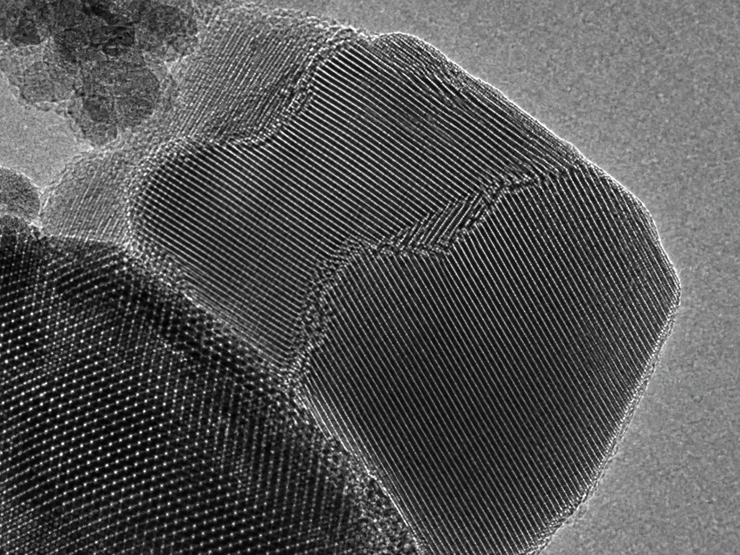
Used to investigate lattice fringes, crystalline domains, interfaces, local defects, and nanoscale crystallographic features.
Selected-area diffraction or complementary TEM modes may be considered where they match the sample and technical objective.
In a transmission electron microscope, an electron beam is accelerated through the microscope column and focused by electromagnetic lenses. The beam passes through a very thin, electron-transparent specimen.
Electrons transmitted through and scattered by the specimen are focused into an image or diffraction pattern. Different lens settings and detectors allow the analysis to reveal morphology, internal structure, crystallinity, lattice features, or interfaces.
Tap a component to see its role in TEM image formation.
The electron source generates the beam and electromagnetic lenses shape it. The beam passes through a thin electron-transparent specimen. Objective and projector lenses form and magnify the transmitted-electron image or diffraction output onto a screen or camera.
High-resolution transmission electron microscopy can reveal lattice fringes and crystalline domains when the specimen, alignment, thickness, and imaging conditions are suitable. These details can help examine crystallinity, interfaces, defects, and local structural changes.
Interpretation depends on the material, orientation, specimen preparation, and imaging conditions. The appropriate output is confirmed during technical review.
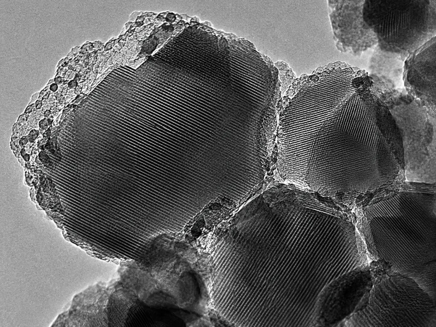
TEM supports research and industrial investigations where nanoscale structure, internal contrast, crystallinity, interfaces, or defects are central to the question being asked.
Particle structure, crystalline domains, interfaces, and degradation features.
Particle morphology, dispersion, agglomeration, and crystalline structure.
Thin interfaces, nanoscale layers, defects, and local structural features.
Layer interfaces, internal morphology, phases, and nanoscale reinforcement.
TEM suitability depends strongly on specimen thickness, preparation, stability, and target information. Share the details first so the appropriate route can be reviewed.
Tell us the material type, expected nanoscale feature, condition, and objective.
Our technical team reviews whether the sample and objective suit the proposed TEM route.
Preparation requirements are discussed before the sample is submitted or dispatched.
Receive the images, observations, and agreed TEM or HRTEM outputs.
TEM analysis is used to investigate nanoscale morphology, internal structure, particle boundaries, interfaces, crystalline regions, lattice features, and defects in thin electron-transparent specimens.
TEM is a broader transmission electron microscopy method that can provide nanoscale imaging and related outputs. HRTEM is a high-resolution mode that may reveal lattice fringes and fine crystalline features when sample and imaging conditions are suitable.
TEM may be suitable for nanoparticles, catalysts, battery materials, thin films, polymers, ceramics, metals, semiconductors, and other specimens that can be made sufficiently thin for electron transmission. Suitability depends on the material and preparation route.
Yes. TEM generally requires a thin, electron-transparent specimen. The preparation route depends on whether the sample is a powder, film, bulk material, cross-section, polymer, or beam-sensitive specimen, and should be confirmed before submission.
TEM imaging primarily reveals morphology and structure. Elemental information may be obtained using complementary techniques such as STEM-EDS or EDX where available and suitable for the sample and analysis objective.
Last reviewed: September 30, 2026
Share a few details for a technical review, or speak directly with our consultant by phone or WhatsApp.
Just a few details — our technical team will guide you.